


Printed Circuit Boards (PCBs) are the fundamental building blocks and nervous system of all modern electronic devices, from consumer smartphones to industrial control systems and aerospace avionics. Their performance, reliability, and miniaturization are paramount. Within the intricate, multi-stage journey of PCB fabrication and assembly, carrier plates (also known as pallets, panels, or fixtures) are indispensable, precision-engineered tools. They are not mere passive supports but active enablers that critically influence the final product's quality, dimensional integrity, manufacturing throughput, and assembly accuracy. Their role is foundational to transitioning from design to mass-produced, functional electronics.
1. Ensuring Dimensional Integrity and Stability During Lamination
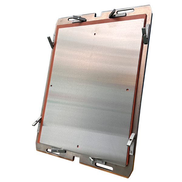
The lamination or hot-pressing process, where multilayer PCB stacks are fused under heat and pressure, subjects the materials to significant thermal and mechanical stress. Without proper support, this can lead to warping, twisting, or bowing—defects that are catastrophic for subsequent high-precision manufacturing steps. Here, carrier plates act as the primary stabilizing substrate. Typically crafted from materials with high thermal conductivity, dimensional stability, and a superior surface finish (such as aluminum composites, steel, or specialized resins), they provide a perfectly flat, rigid foundation.
During pressing, the PCB stack is securely placed on or between these plates. The plates evenly distribute the immense press tonnage across the entire panel area, preventing localized stress points that could cause deformation. Simultaneously, their thermal properties help conduct heat uniformly from the press platens, mitigating thermal gradients that are a primary cause of warpage. By constraining the PCB in a perfectly planar state throughout the curing cycle, carrier plates ensure the final product meets stringent flatness specifications. This dimensional stability is non-negotiable for the success of later processes like automated solder paste application, high-speed component placement, and precise optical inspection, all of which rely on a perfectly flat board.
2. Maximizing Production Efficiency Through Panelization and Batch Processing
Modern electronics manufacturing is driven by economies of scale and throughput. Carrier plates are the engine of this efficiency in the PCB fabrication stage. The practice of panelization—where multiple individual PCB units (or "cards") are arrayed onto a single, larger carrier plate—is standard. This master panel, secured to the carrier plate, undergoes lamination, imaging, plating, and routing as a single entity.
The benefits are substantial. Batch processing dozens or even hundreds of PCBs simultaneously drastically increases throughput per press cycle, directly boosting production capacity and reducing unit cost. It minimizes the handling of individual, fragile boards, lowering the risk of mechanical damage. Furthermore, it standardizes the process, reducing the variability and potential for error associated with handling numerous small pieces. The carrier plate also provides essential tooling holes and fiducial marks that automate the panel's precise alignment and registration through different machines (drills, plotters, etc.), streamlining the entire workflow. After all processes are complete, the individual PCBs are simply depanelized (routed or scored out), leaving behind a highly efficient batch of finished boards.
3. Guaranteeing Assembly Accuracy and Enhancing Final Product Reliability
The transition from a bare PCB to a populated, functional assembly is perhaps the most critical phase. Here, carrier plates evolve from fabrication aids to precision assembly fixtures, especially in Surface Mount Technology (SMT) lines. In this role, they are often custom-machined to securely hold one or more PCBs, complete with precise cutouts, locator pins, and clamping mechanisms.
This fixture provides unwavering mechanical stability as the board travels at high speeds through printers, placement machines, and reflow ovens. It eliminates vibration, flexing, or positional drift, which are primary causes of misaligned components, skewed solder paste deposits, and poor solder joint formation. For double-sided assembly or complex assemblies, the carrier plate ensures the board remains perfectly flat, allowing both sides to be populated with micron-level accuracy. This precise constraint is crucial for components with fine pitches, such as Ball Grid Arrays (BGAs) or chip-scale packages, where even minor board deviation can lead to open or short circuits.
By ensuring flawless component placement and soldering, the carrier plate directly contributes to the final product's functional reliability, electrical performance, and longevity. It reduces defects, minimizes rework, and ensures that every unit performs as designed, upholding quality standards in highly competitive and reliability-sensitive markets.
Conclusion
In essence, carrier plates are the silent orchestrators of precision and scale in PCB manufacturing. They bridge the gap between the fragility of raw laminate materials and the rugged demands of high-volume, automated production. From ensuring a warp-free board fresh from the lamination press, to enabling the batch processing that makes mass production viable, to providing the rock-solid platform for perfect component assembly, their role is comprehensive. Investing in high-quality, precisely engineered carrier plates is not an overhead but a strategic imperative—a direct investment in yield, throughput, consistency, and, ultimately, the performance and reliability of the electronic devices that power the modern world.
