Mass Lam vs. Pin Lam in PCB Lamination: Key Differences, Requirements & Best Practices
In multilayer printed circuit board (PCB) fabrication, the lamination process is pivotal to ensuring structural integrity, electrical performance, and interlayer alignment accuracy. Two dominant tooling methodologies are employed to maintain registration during this high-temperature, high-pressure phase: Mass Lam (pinless lamination) and Pin Lam (pinned lamination). Understanding their distinctions is essential for PCB designers and manufacturers aiming to balance precision, cost, throughput, and reliability.
This article breaks down the technical differences, application scenarios, equipment requirements, and selection criteria—complete with SEO-optimized insights for engineers and procurement professionals in the electronics manufacturing industry.
What Is Pin Lam (Pinned Lamination)?
Pin Lam uses precision-drilled registration holes in steel plates, inner-layer cores, and release films. High-temperature-resistant pins—typically made of ceramic or hardened steel—are inserted through the entire stack before lamination to mechanically lock layers in place.
Key Features of Pin Lam:
High alignment accuracy: ±15–25 μm
Ideal for HDI PCBs, high-layer-count boards (>12 layers), rigid-flex, and IC substrates
Requires dedicated pinning and de-pinning stations
Higher operational cost due to pin wear, maintenance, and extra handling
Longer setup time but superior registration control
Best for: Applications where layer-to-layer registration tolerance is critical, such as 5G infrastructure, aerospace, and advanced packaging.
What Is Mass Lam (Pinless Lamination)?
Mass Lam eliminates mechanical pins entirely. Instead, it relies on:
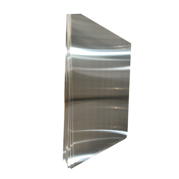
Ultra-flat lamination steel plates (flatness ≤5 μm)
Precision press platen parallelism
Symmetrical inner-layer design
Controlled resin flow dynamics during cure
Key Features of Mass Lam:
Simplified workflow: No drilling or pin insertion/removal
Typical alignment accuracy: ±30–50 μm (advanced systems achieve ±30 μm)
Lower material and labor costs
Higher throughput and better suited for automation
Demands strict control over material symmetry and press uniformity
Best for: High-volume production of standard multilayer PCBs (4–16 layers), such as consumer electronics, networking hardware, and industrial controllers.
Mass Lam vs. Pin Lam: Side-by-Side Comparison
Parameter | Pin Lam | Mass Lam |
|---|---|---|
Registration Accuracy | ±15–25 μm | ±30–50 μm |
Ideal Layer Count | 8+ layers (especially >12) | 4–16 layers |
HDI / Microvia Support | Excellent | Limited (requires evaluation) |
Steel Plate Requirement | Must be drilled; high hole precision | Ultra-flat (≤5 μm), distortion-free |
Press Requirements | Standard | High parallelism, uniform heat/pressure |
Production Throughput | Lower (manual pin handling) | Higher (fully automatable) |
Total Cost | Higher (pins, labor, maintenance) | Lower (leaner process) |
How to Choose Between Mass Lam and Pin Lam?
Selecting the right lamination method depends on your product’s technical and economic profile:
✅ Choose Pin Lam if:
Your design requires tight layer alignment (≤25 μm)
You’re producing HDI, RF, or rigid-flex PCBs
Yield and reliability outweigh cost concerns
✅ Choose Mass Lam if:
You’re manufacturing high-volume standard multilayer boards
You prioritize cost efficiency and automation
Your design has symmetrical layer stackups and moderate alignment tolerance
Pro Tip: Modern Mass Lam systems—paired with advanced dielectric materials and AI-assisted press control—are closing the precision gap. Evaluate your manufacturer’s capabilities before defaulting to Pin Lam.
Neither Mass Lam nor Pin Lam is universally superior—each excels in its niche. As PCB technology advances, Mass Lam adoption is growing in mid-tier applications thanks to improvements in steel plate flatness, press control, and material science. However, Pin Lam remains indispensable for ultra-high-precision sectors.
For PCB fabricators, the key is aligning your lamination strategy with your product roadmap, quality standards, and automation goals. Partner with a manufacturer who offers both capabilities—and the engineering expertise to recommend the optimal path.


