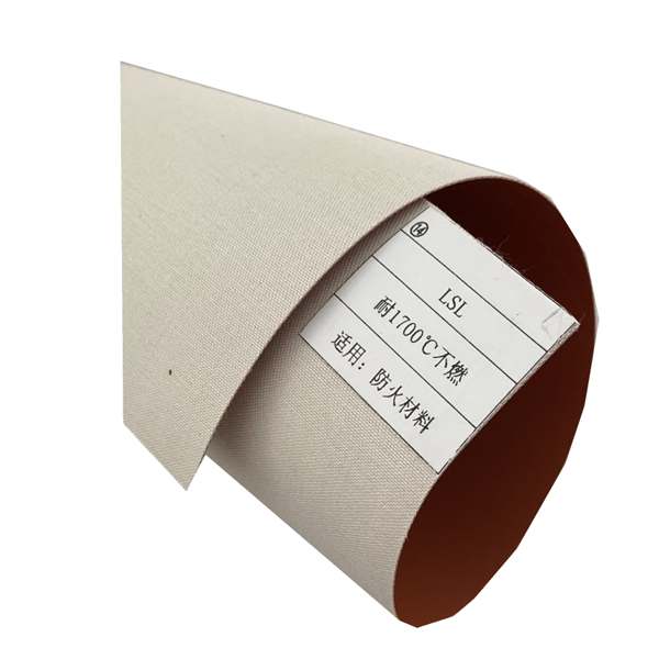
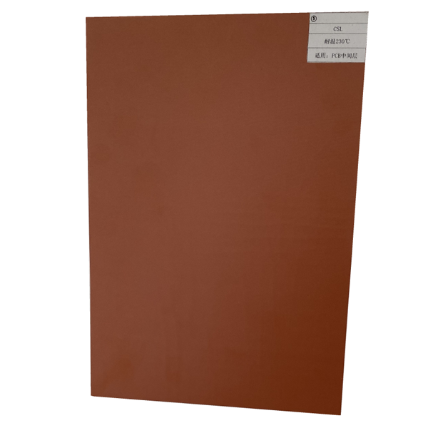
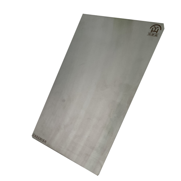
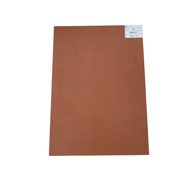
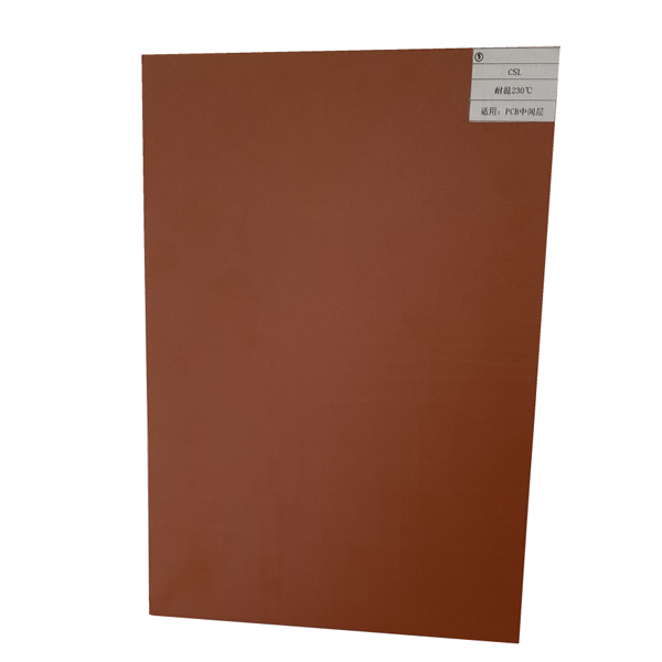
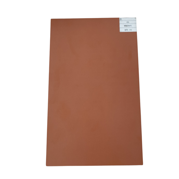
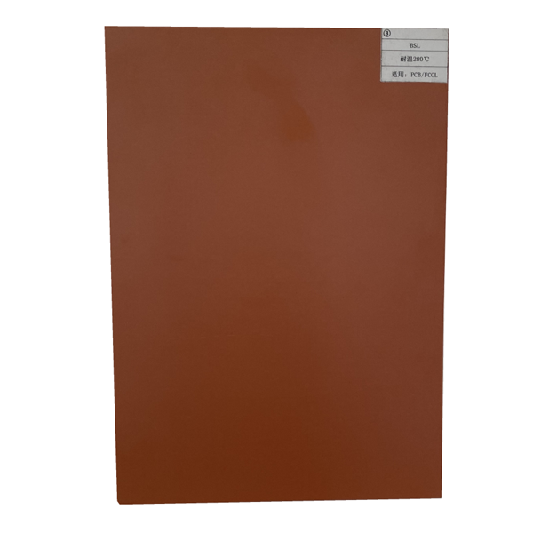
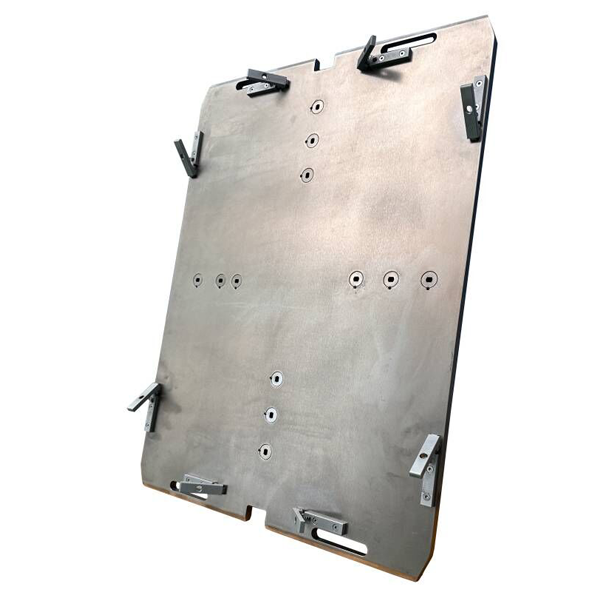
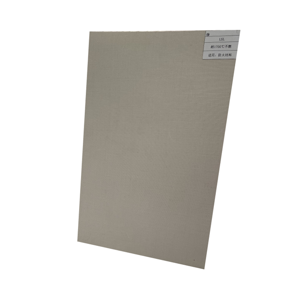
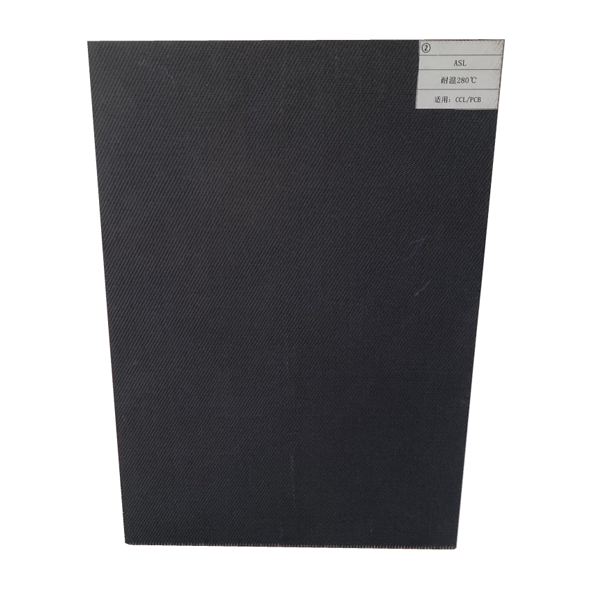
In the manufacturing process of printed circuit boards (PCB), the lamination process is a key step that determines the quality of multilayer boards. As a professional PCB buffer pad manufacturer, we understand the significant impact of high-quality buffer pads on PCB lamination quality. This article will comprehensively introduce the functional characteristics, product advantages, and how to choose an excellent supplier of PCB buffer pads, helping PCB manufacturers improve production efficiency and product quality.
The Core Role of PCB Buffer Pads in Multilayer Board Lamination
PCB Buffer Pads are key auxiliary materials placed between the heat press plate and the PCB board to be pressed, primarily functioning to ensure even distribution of pressure and temperature during the lamination process. As an experienced PCB buffer pad manufacturer, our buffer pads can:
Evenly distribute pressure: Eliminate localized overpressure that may cause deformation of the inner layers or damage to the circuit lines of the PCB
Stable heat transfer performance: Ensure even heat distribution during lamination, avoiding localized overheating or insufficient curing
Protect expensive equipment: Reduce equipment wear caused by direct contact between the heat press plate and the PCB board
Improving yield rate: Significantly reduce the rate of defective boards caused by pressing issues through a stable pressing environment
Adapting to diverse needs: Meet the pressing requirements for PCB boards with different numbers of layers and thicknesses
Product advantages of professional PCB buffer pad manufacturer
As a leading domestic PCB buffer pad manufacturer, our products have a high reputation in the industry, with main advantages reflected in the following aspects:
1. Carefully selected special materials to ensure excellent performance
We use imported high polymer composite materials, which have been strictly screened and tested to ensure they have:
Excellent heat resistance (long-term operating temperature can reach above 300℃)
Stable compression rebound characteristics (rebound rate > 90%)
Uniform density distribution (density deviation < ±1.5%)
Excellent anti-aging performance (service life can reach 100-150 cycles of lamination)
Very low thermal expansion coefficient (<30×10⁻⁶/℃)
2. Precision manufacturing process to ensure product consistency
By introducing German CNC machining centers and Japanese precision testing equipment, we have achieved:
Thickness tolerance is controlled within ±0.015mm for ultra-high precision
Surface flatness reaches Ra<0.2μm, industry-leading level
Edge processing uses laser cutting technology to ensure no burrs and no delamination
Performance variation between batches is controlled within 3%
Custom non-standard manufacturing supported, with fastest 3-day delivery for special specification products
3. Strict quality control system
We have established a quality control system that runs throughout the entire process:
72-hour aging test for raw materials
Sampling inspection every 2 hours during production
100% full inspection for finished products, with double confirmation of key parameters
Performance verification by third-party laboratory every month
Complete traceable quality records are kept for more than 3 years
Key Applications of PCB Buffer Pads in Multilayer Board Production
As a professional PCB buffer pad manufacturer, we deeply understand the process requirements of different PCB products:
1. Pressing of Ordinary FR-4 Multilayer Boards
For conventional FR-4 materials, our buffer pads can effectively:
Evenly distributed interlayer pressure for 6-20 layer boards
Ensure sufficient resin flow and complete curing
Reduce lamination slippage (controlled to <0.3mm)
Decrease board warping after lamination (warping degree <0.5%)
2. Laminating for High Frequency and High Speed Boards
For special materials such as PTFE, we provide:
Specialized low dielectric constant buffer pads
Optimized surface treatment to prevent material adhesion
Precision temperature control design prevents damage to high-frequency materials
Special anti-static treatment
3. HDI high-density interconnect board lamination
For the demand of fine circuit lines, we have developed:
Precision Surface Buffer Pads (Ra<0.1μm)
Microporous Breathable Design
Ultra-Thin Specifications (0.3-0.5mm)
Low Thermal Expansion Series
4. Thick Copper Board/Metal Base Lamination
For special structure boards, we provide:
High Compression Strength Buffer Pads (>50MPa)
Enhanced Thermal Conductive Design
Edge reinforcement treatment
High-temperature resistant special models
How to choose a reliable PCB buffer pad manufacturer
Selecting a high-quality PCB buffer pad manufacturer should focus on the following aspects:
Technical Expertise:
Does the company have a material R&D laboratory?
Can you provide a detailed technical parameters report
Do you understand the characteristics of PCB production processes
Production Equipment Level:
Precision grade of processing equipment
Advanced Testing Equipment
Automation Production Level
Quality Assurance System:
Whether it has passed ISO9001 certification and other certifications
Is the quality control process complete?
How traceable is the product?
Industry Service Experience
Case Studies of Serving Well-Known PCB Companies
Ability to Handle Special Requirements
Technical Response Speed
Cost-Effectiveness Evaluation
Single Use Cost Calculation
Lifespan Comparison
Contributions to yield improvement
As a professional PCB buffer pad manufacturer with 15 years of deep industry experience, we have obvious advantages in all the above aspects and have served more than 200 PCB production enterprises, including several listed companies and foreign-funded enterprises.
Our Service Commitment
Choosing us as your PCB buffer pad supplier, you will get:
Free Technical Consultation: Provide press-fit process optimization solutions
Sample Testing Support: Can provide comparative testing for different specifications
Urgent Order Response: Standard products are shipped within 24 hours
Regular Performance Monitoring: Track product usage data and provide optimization suggestions
Professional Technical Training: Regularly hold PCB lamination technology seminars
After-sales Rapid Response: Professional engineers provide technical support within 12 hours
We understand that although PCB buffer pads are small, they have a significant impact on product quality. Therefore, we always adhere to the goal of "zero defects," continuously improving product performance and service quality to create the maximum value for our customers.
Contact Us
If you are looking for a reliable PCB buffer pad manufacturer, or wish to optimize your existing lamination process, feel free to contact us at any time.


