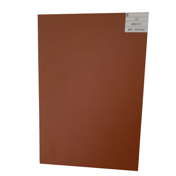
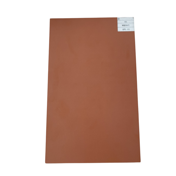
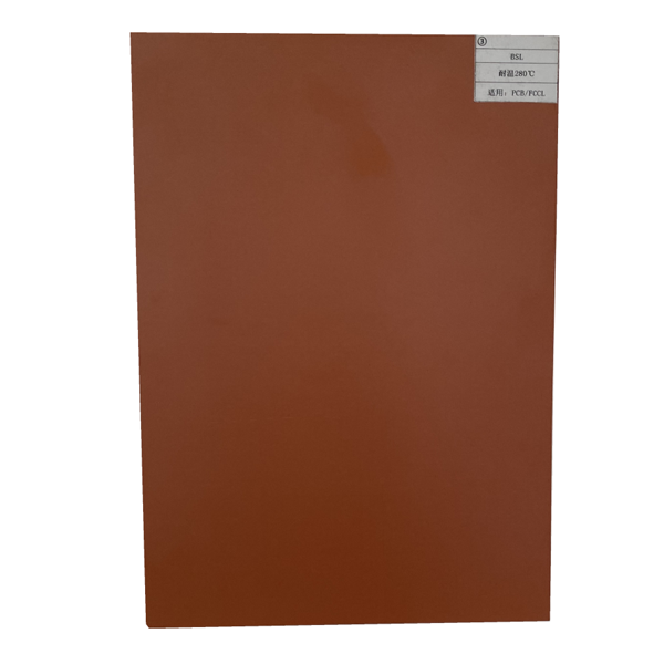
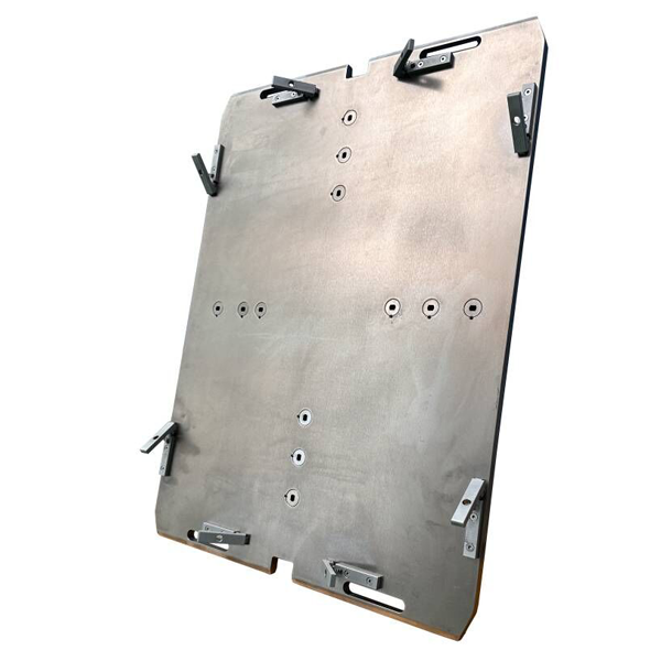
What is a PCB Lamination Buffer Pad
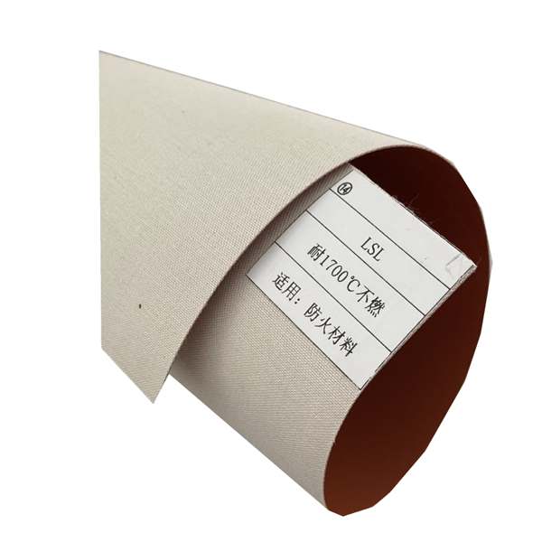
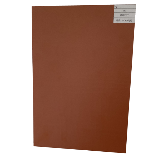
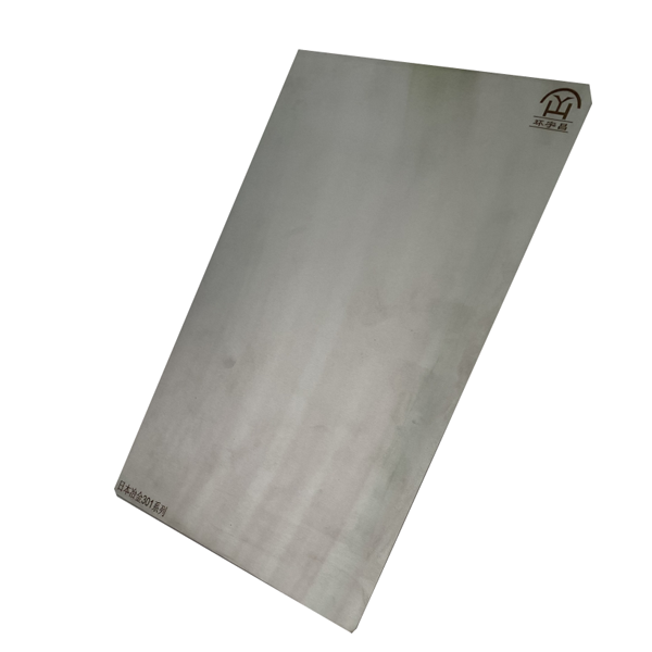
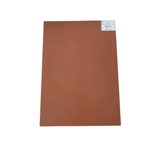
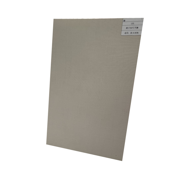
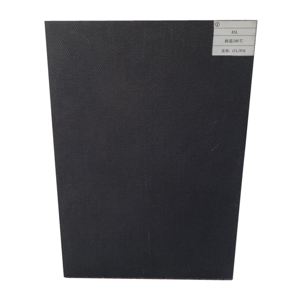
The PCB lamination buffer pad is an essential auxiliary material in the printed circuit board (PCB) manufacturing process, primarily used in the lamination process of multilayer circuit boards. During the high-temperature and high-pressure lamination process, the buffer pad plays an important role in evenly distributing pressure, protecting the copper foil surface, and regulating heat transfer.
As a professional manufacturer of press cushion pads, we fully understand the impact of this material on the final quality of PCB products. High-quality cushion pads can significantly reduce the defect rate during the pressing process, improve product yield, and lower production costs.
Core Function of PCB Press Cushion Pads
Even Pressure Distribution
Multi-layer PCBs require extremely high pressure (usually reaching 300-500psi) during the pressing process. The primary function of cushion pads is to evenly distribute the pressure from the press across the entire board surface, preventing quality issues caused by excessive or insufficient pressure in certain areas.
Our laboratory test data shows that using high-quality buffer pads can improve pressure distribution uniformity by more than 40%, effectively reducing issues such as interlayer misalignment and bubbles caused by uneven pressure.
Surface protection
PCB lamination buffer pads act as a protective layer under high-temperature and high-pressure conditions, preventing the press plate from directly contacting the copper foil surface and causing scratches or dents. Especially for high-precision HDI boards, the requirement for surface flatness is extremely high, making the protective role of buffer pads even more critical.
Temperature regulation function
Buffer pad materials have specific thermal conductivity properties that can regulate the heat transfer speed in PCB boards, ensuring even curing of the resin across all layers. This characteristic is particularly important for the manufacturing of special PCBs such as thick copper boards and high-frequency boards.
Buffer pad material properties
High-temperature resistance
High-quality PCB buffer pads must be able to withstand high-temperature environments above 200°C and maintain stable performance even after multiple lamination cycles. We use specially treated aramid fiber materials with a heat resistance up to 300°C, meeting the requirements of various high-end PCB manufacturing applications.
Elastic Recovery Ability
Good elasticity is a core performance indicator of the buffer pad. Our products are processed through special techniques, achieving a compression rebound rate of over 85%, ensuring stable buffering performance even after multiple press operations and significantly extending service life.
Low Thermal Expansion Coefficient
To prevent dimensional instability caused by temperature changes, our buffer pad material has an extremely low coefficient of thermal expansion (CTE). The dimensional change is less than 0.5% in high-temperature environments, ensuring accurate pressing.
How to choose the suitable PCB lamination buffer pad
Selecting based on PCB type
Different types of PCB have varying requirements for buffer pads:
Standard multilayer boards: standard buffer pads can meet the needs
HDI high density board: special buffer pads with high flatness and low impurity content should be selected
High frequency board: requires special materials with low dielectric loss
Thick copper board: needs enhanced buffer pads with higher pressure resistance
Consider the lamination process parameters
When selecting a buffer pad, it is necessary to consider comprehensive process parameters such as pressing temperature, pressure, and time. Our technical team can recommend the most suitable buffer pad specifications and models based on the customer's specific process conditions.
Balancing service life and economy
Although high-quality buffer pads have a higher unit price, their long service life results in a lower overall cost. We recommend that customers do not only focus on the initial purchase cost but should calculate the cost per pressing cycle to choose the most economical product.
Usage and maintenance of pressing buffer pads
Correct Usage Method
To ensure optimal performance, when using the buffer pad, pay attention to the following:
Maintain a clean working environment to prevent contamination from impurities
Regularly rotate the position of the buffer pad to evenly distribute wear
Control appropriate pre-press time to extend service life
Key points for daily maintenance
We recommend that customers establish a buffer pad maintenance record, documenting:
Number of uses and lamination parameters
Surface Condition Inspection Results
Cleaning and Maintenance Records
Performance Test Data
Regular professional inspections can detect the performance degradation of the buffer pads in advance, preventing PCB quality issues caused by material aging.
Future Development Trends
As PCB technology advances towards high density and high frequency, the requirements for bonding pads are becoming increasingly stringent. As a professional manufacturer, we are committed to:
Developing new materials with lower thermal expansion
Enhancing the durability and stability of the bonding pads
Optimize surface treatment technology to reduce transfer contamination
Develop environmentally friendly and recyclable buffer pad materials
PCB press buffer pads, though a small material, have a significant impact on the quality of circuit board manufacturing. Choosing a professional press buffer pad manufacturer to obtain high-quality products and technical support is an effective way to improve PCB production yield and reduce overall costs.


