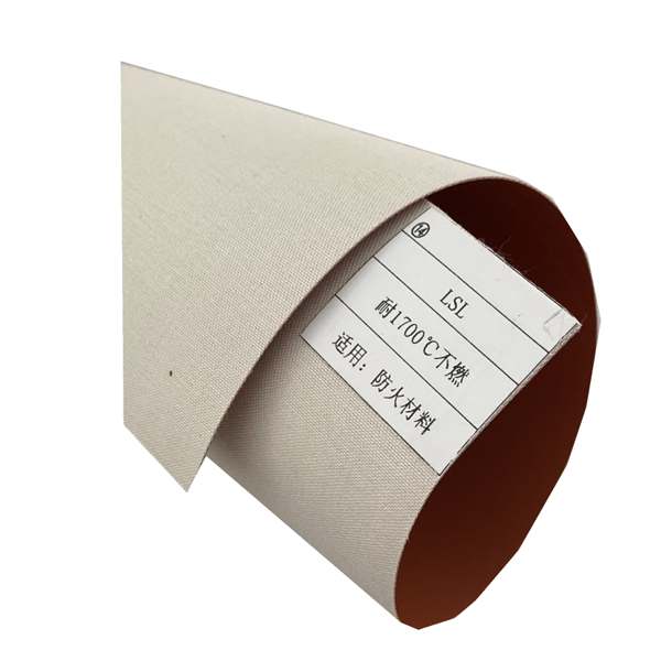
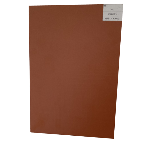
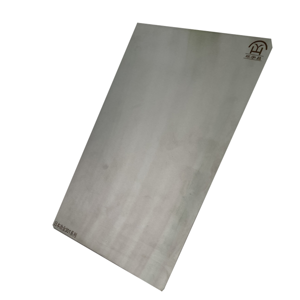
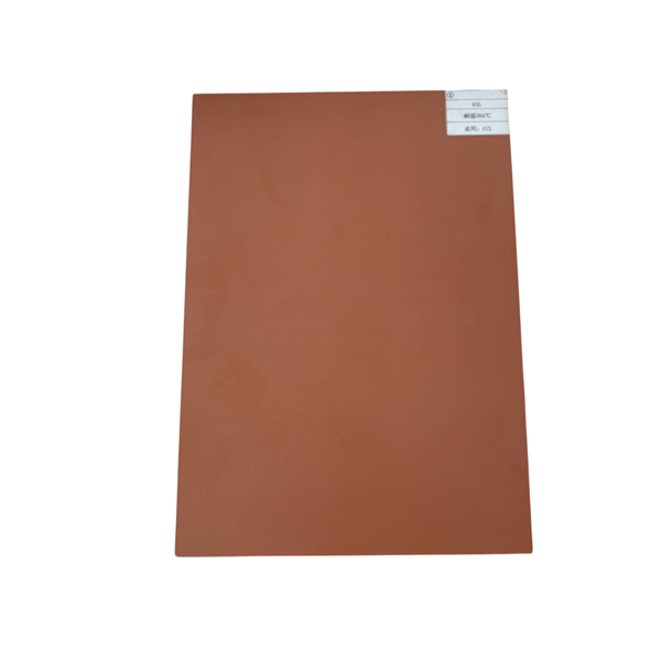
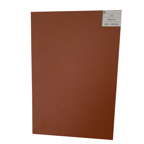
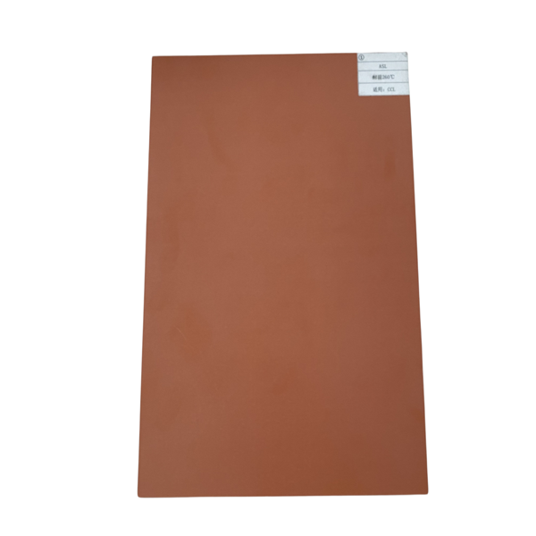
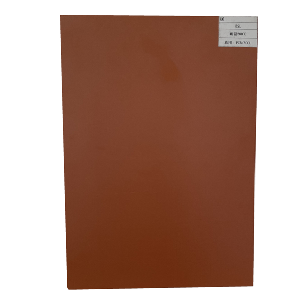
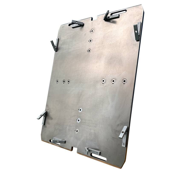
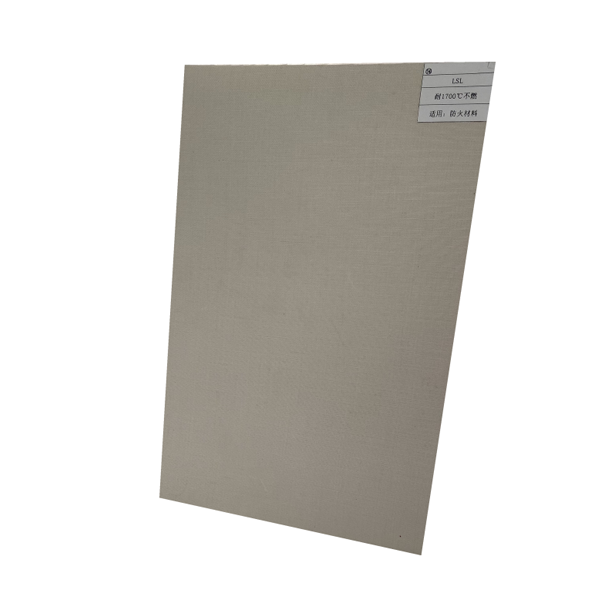
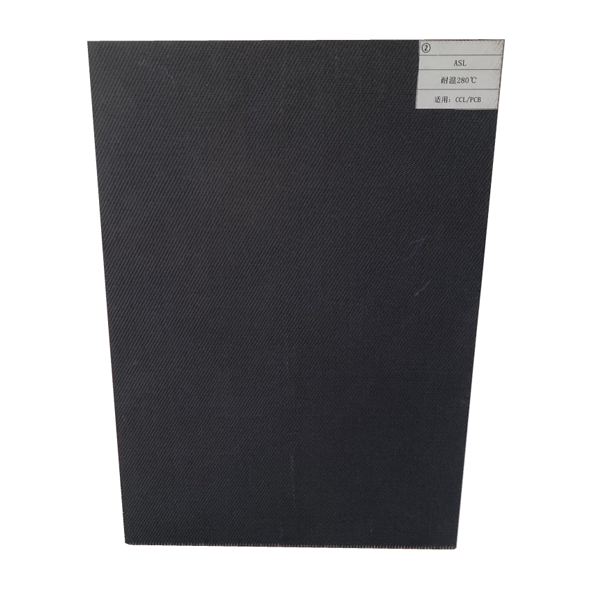
In the manufacturing process of electronic base materials such as PCB (Printed Circuit Board), FPC (Flexible Printed Circuit), and CCL (Copper Clad Laminate), the pressing process directly determines the interlayer bonding strength, dimensional stability, and electrical performance of the finished board. As a professional buffer pad manufacturer, we will delve into the core functions, technical parameters, and selection criteria of PCB pressing buffer pads, helping customers achieve higher quality pressing processes.
One, Core Function of PCB Pressing Buffer Pads
Even Pressure Distribution
By elastic deformation, the buffer pads absorb pressure fluctuations from the press, preventing excessive local pressure that could cause deformation of inner layers or uneven thickness of the dielectric layers. Experimental data show that high-quality buffer pads can control pressure differences on the pressing working surface within ±5%.Temperature Conduction Optimization
Special silicone composite materials enable rapid heat conduction, shortening the heating time (efficiency improved by 20-30% compared to traditional materials), while also preventing overheating damage to copper foils.Surface Defect Protection
The 3D microporous structure can effectively adsorb gases and volatile substances generated during the lamination process, preventing the occurrence of defects such as pits and white spots on the PCB surface.
II. Technical Parameter Analysis (Industry Leading Standards)
| Parameter Items | Standard value range | Test method |
|---|---|---|
| Heat resistance | -50℃~300℃ | ASTM D573 |
| Compression rebound rate | ≥92% (200 cycles) | ISO 1856 |
| Tear Strength | ≥35KN/m | ASTM D624 |
| Thickness Tolerance | ±0.05mm | Laser thickness gauge |
| Thermal conductivity | 0.8-1.2W/mK | ASTM E1461 |
Three. Dedicated Solutions for Different Materials
Rigid PCB Lamination
High-density composite buffer pads are recommended, as their anti-crawling properties can meet the long-term lamination needs of boards with 4-32 layers, especially suitable for HDI board manufacturing.FPC Flexible Board Lamination
Specialized Flexible Pad, using ultra-fine fiber reinforced structure, maintains cushioning performance while preventing transfer of impressions, with surface roughness controlled at Ra ≤ 0.2 μm.High Frequency Material Lamination
Low Dielectric Constant Version, which reduces signal transmission loss, with dielectric constant stable at 2.8-3.2 (under 1MHz conditions).
Four. Common Issues and Solutions
Q1: What should be done if the buffer pad surface shows indentation?
→ It is usually caused by exceeding the service life (recommended to replace after 500 press cycles) or temperature overruns. We recommend using our thickness monitoring system in conjunction.
Q2: How to choose the appropriate hardness?
→ Reference formula: Hardness (Shore A) = (Pressing pressure MPa × 15) + 20, for example, 8MPa pressure corresponds to 140Shore A.
Q3: How to improve board edge warping after lamination?
→ It is necessary to check the thermal expansion coefficient compatibility of the buffer pad. Our CTE customization service can precisely control the material's expansion in the XY direction ≤15ppm/℃.
Five、Production Process Advantages
Using imported automated production lines to achieve:
Nano-level filler uniform dispersion technology
Online X-ray inspection to ensure no bubble defects
Independent QR code traceability system for each roll of material
Six. Customer Case Studies
A Yield Improvement Solution for a Listed PCB Enterprise
Original Situation: Panel bonding process yield is 89.7%, with monthly scrap loss of approximately 230,000 yuan
Solution: Replaced with our company's release film combination solution
Effectiveness:
✓ Yield improved to 96.3%
✓ Buffer pad service life extended by 40%
✓ Annual cost savings exceed 1.8 million yuan
Why choose our PCB laminating buffer pads?
15 years dedicated to electronic material buffer solutions
Passed UL94 V-0 certification, compliant with RoHS 2.0 standard
Support 48-hour sample fast shipping service
Provide guidance on optimizing lamination process parameters
Get free technical consultation immediately


