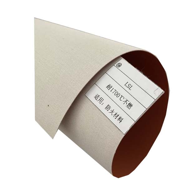
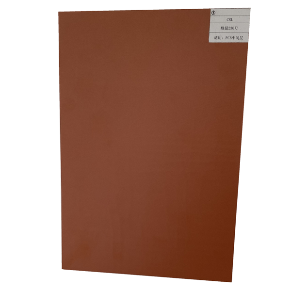
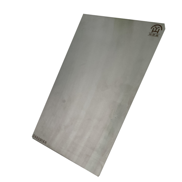
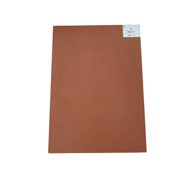
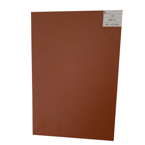
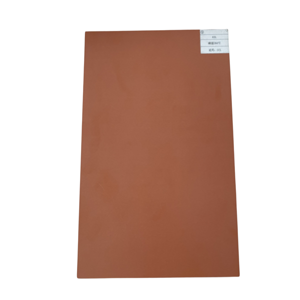
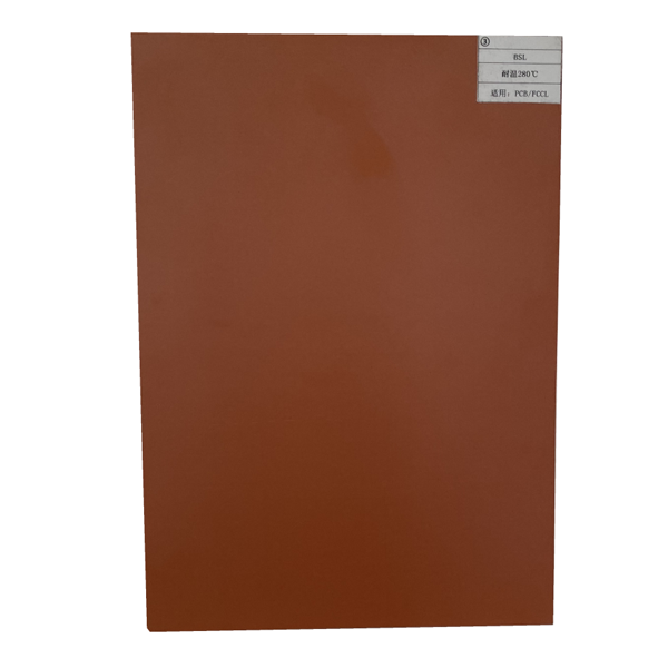
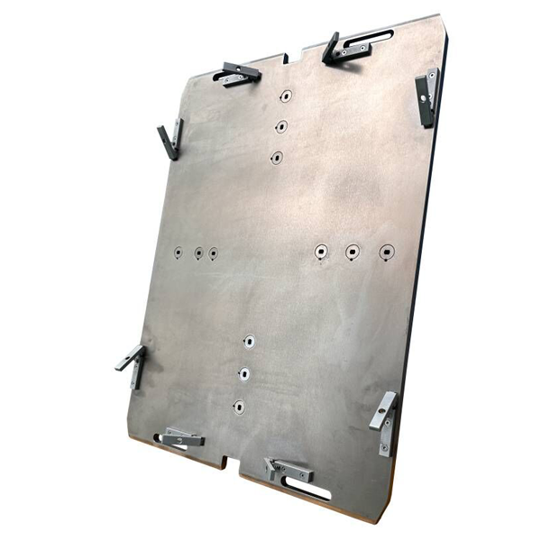
In the world of precision manufacturing of printed circuit boards (PCB), every step is crucial to the success or failure of the final product. Among these steps, the "pressing" process is undoubtedly the core and soul of multilayer board production. Within this harsh environment of high pressure and high temperature, there is a silent yet vital "guardian"—PCB Pressing Buffer Pads.
Today, we visit a well-known domestic PCB Pressing Buffer Pads manufacturer—Henan Huanyuchang Electronic Technology Co., Ltd.—and have an in-depth conversation with their technical experts, revealing the technological secrets behind this small material and how it becomes a key factor in determining the quality of PCBs.
What is a PCB press cushion and why is it indispensable?
Before diving deeper, we need to clarify a basic concept: what is a PCB press cushion?
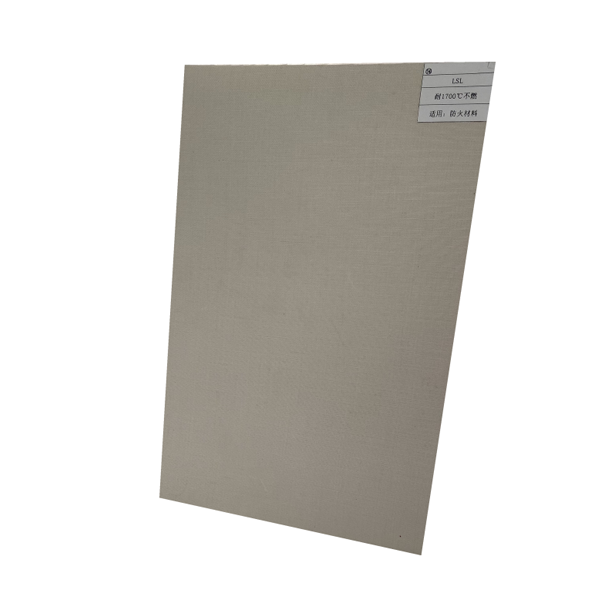
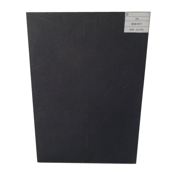
In simple terms, a PCB press cushion is a special composite material placed between the hot press plate of the press machine and the PCB copper foil and pre-impregnated sheets (PP) being pressed. It is usually made of kraft paper, fiber cotton, or other high-performance synthetic materials, and has characteristics such as high heat resistance, high pressure resistance, good elastic recovery, and uniform heat conduction.
"Many people outside the industry, even some beginners in the PCB field, may underestimate the role of buffer pad," explained Wang Gong, the technical director of Henan Huanyuchang. "Its function is similar to a soft diffuser that a professional photographer places in front of a softbox. Without it, the light (heat and pressure) would directly and harshly hit the object, leading to uneven exposure and loss of details. The PCB press cushion, on the other hand, is responsible for converting the rigid pressure and heat generated by the press into a uniform, gentle, and stable 'force field' that fully wraps around the circuit board during the pressing process."
So, what are the essential roles that this "guardian" plays?
Even pressure distribution: When multi-layer boards are laminated, their surfaces are not absolutely flat. The unevenness of the circuit lines can lead to localized pressure concentration. Buffer pad can fill these microscopic irregularities through its elastic deformation, ensuring that pressure is evenly transmitted to every corner of the board, thus preventing defects such as insufficient resin filling, bubbles (white spots), and sliding board caused by uneven pressure.
Heat balance conduction: Modern lamination processes have very strict requirements for temperature profiles. PCB lamination buffer pad has good thermal conductivity, which helps in quickly and evenly distributing heat across the entire board area, ensuring that all regions of the pre-impregnated material reach the melting and curing temperature almost simultaneously, thus achieving consistent resin flow and curing degree.
Absorbing stress and impurities: During the lamination process, resin may overflow, or there may be tiny particles in the stack. Buffer pad can effectively absorb the overflowed resin and accommodate these small impurities, preventing them from damaging the expensive, highly polished hot pressing plates of the laminator, and also avoiding these impurities from scratching the surface of the PCB under pressure.
Compensation for thickness tolerance: Different batches of pre-impregnated sheets or core boards may have slight thickness variations. The compressibility of the buffer pad can effectively compensate for these tolerances, ensuring the final multilayer board has consistent thickness and meets the customer's strict specifications.
II. Quality is just a thought away: Chain of disasters caused by inferior buffer pads
"Choosing a low-quality or incompatible PCB lamination buffer pad is undoubtedly the beginning of a disaster for PCB manufacturers," Wang Gong's tone became serious. He listed several common issues:
Lamination white spots/bubbles: This is the most common problem. Inferior buffer pads with uneven elasticity or poor recovery properties cannot effectively fill the gaps between circuits, leading to poor resin flow, localized lack of adhesive, and the formation of white spots or bubbles, which severely affect the interlayer bonding strength and electrical reliability.
Panel warping and deformation: Uneven pressure and heat conduction can cause internal stress differences in different areas of the panel. After lamination, these internal stresses are released, leading to warping and twisting of the panel, which brings significant difficulties to subsequent SMT mounting and may even result in scrapping.
Surface pits and pinholes: If the material of the buffer pad is impure and contains hard particles or impurities, these contaminants can leave pits or pinholes on the copper foil surface under hundreds of tons of pressure, damaging the integrity of the conductor and easily causing signal transmission issues in high-frequency and high-speed circuits.
Sliding and misalignment between layers: Mismatched friction coefficients of the buffer pad may lead to relative sliding of the materials under high pressure, causing misalignment between layers and directly resulting in the panel being scrapped.
Damage to the press plate: Poor-quality buffer pad may decompose and stick to the plate under high temperature, and the impurities it contains can scratch and contaminate the hot press plate. The cost of replacing or repairing the hot press plate is extremely high, and the production downtime losses are even more incalculable.
Therefore, Henan Huanyuchang has always emphasized to its customers that PCB lamination buffer pad is far from an ordinary consumable; it is a key "process material" in the lamination process. Its cost accounts for a very small portion of the total board cost, but its impact on yield, efficiency, and cost is decisive.
Three. Henan Huanyuchang's Craftsmanship Approach: How to Create a Good PCB Lamination Buffer Pad
As a professional PCB lamination buffer pad manufacturer, Henan Huanyuchang knows well the responsibility they bear. They have established a strict quality control system from raw materials to finished products.
1. Raw Material Selection and Formula Optimization:
"We only collaborate with global high-quality raw material suppliers," said Wang Gong. "From imported long-fiber pulp kraft paper to special temperature-resistant polymers, every roll of raw material undergoes strict incoming inspection." Henan Huanyuchang has its own material laboratory, and has developed various formulas of buffer pad to meet the needs of different PCB types, such as high-speed high-frequency boards, HDI boards, metal base boards, and thick copper boards, ensuring different thermal conductivity, compression rate, rebound properties, and temperature resistance requirements are satisfied.
2. Precise production process:
In the production workshop, we saw the fully automatic production line running smoothly. From the impregnation of original paper, coating with special reagents, to high-temperature drying and calendering for flatness, every process parameter is precisely controlled. "Temperature and tension are the core," said Wang Gong, pointing at a drying machine. "We ensure that the buffer pad undergoes 'pre-stabilization' treatment during manufacturing, making it more stable and longer-lasting in the customer's laminator, reducing the frequency of replacement."
3. Comprehensive product testing:
Before leaving the factory, each roll of PCB press cushion from Henan Huanyuchang must undergo a "health check." The testing items include:
Thickness and uniformity testing: Ensuring the thickness tolerance is controlled at the micrometer level.
Quantum and density testing: Guaranteeing consistency between batches.
Tensile strength and elongation: Ensure it does not tear easily under high pressure.
Thermal stability and weight loss test: Simulate the high-temperature environment of lamination to detect volatile content and decomposition rate, ensuring no residue and no sticking to the board.
Compression rebound rate test: This is a core indicator, directly related to the performance of pressure uniformity.
Four: Looking Ahead - Henan Huanyuchang and PCB Technology Grow Together
With the rapid development of 5G communication, artificial intelligence, the Internet of Things, and automotive electronics technology, PCBs are evolving towards higher density, higher frequency, and higher reliability. This presents unprecedented challenges for PCB lamination buffer pads.
"For example, ultra-thin multilayer boards used for IC carriers have extremely fine circuits, requiring pressure uniformity at the nanometer level. Meanwhile, buffer pads used for large-sized server boards need to have exceptional thermal conductivity and thickness consistency across the entire large area," said Wang Gong. "Henan Huanyuchang has been proactive. Our R&D team is currently working on the next generation of nano-porous structure buffer pad materials, aiming to achieve lower thermal resistance, more precise elastic modulus, and longer service life to keep up with the future development of the PCB industry."
Conclusion
In the field of precision manufacturing, details determine the height. PCB press laminating buffer pad, this seemingly ordinary material, is actually the cornerstone of the quality of PCB laminating. Choosing a reliable, professional, and technically leading partner means injecting stability and reliability into your production line.
Henan Huanyu Chang Electronic Technology Co., Ltd. is committed to becoming the most trusted "pressure bonding guardian" for global PCB manufacturers, leveraging its deep understanding of materials, relentless pursuit of craftsmanship, and unwavering commitment to quality. They provide not just a PCB pressure bonding pad, but a solid guarantee for the quality of their customers' products.


